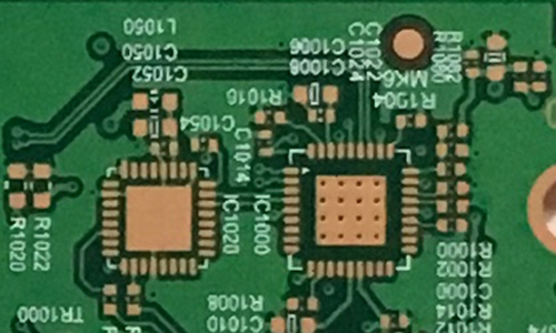
Gold Immersion Multilayer PCB Board for ASIC Communication Printed Circuit Board
The Multilayer PCB Board is applied to communication device, which is a 4 layers multilayer PCB board. The specification of the PCB board is 37 * 37 mm, with green solder mask and OSP surface treatment.
What We Can Do for You?
With over 18 years experience, we offer OEM & ODM PCB Layout, PCB Design, PCB manufacturing and
PCB Assembly in single-sided PCB Board, double-sided PCB and Multilayer Printed Circuit Board service to
our customers, with total production capacity of 290,000 sqm/month.
How to get quick quotation?

| Step 1 Please send us Gerber file with these format: .CAD / .Gerber / .PCB / .DXP / .P-CAD, etc |
| Step 2 Also please provide us the below details for quick quotation: |
|
Board material: Fr - 4 / CEM - 1 / CEM - 3 / 22F / Fr - 1 / others
|
| Material brand: SY / KB / Rogers (optional) |
| Material Specification:High Tg / copper based / aluminum based or others (optional) |
| Board thickness: 0.1 - 6.0 mm |
| Copper thickness: 0.05 Oz - 8 Oz ( 17 um - 288 um ) |
| Surface Treatment: OSP / ENIG / HASL / Lead Free HASL / Immersion Tin / Immersion Sin |
| Color of solder mask and silk print: Green / red / blue / black / white / yellow ,etc |
| Board size and quantity |
|
If you don't have Gerber file, please provide us the imfomation as step 2 or post your PCB Board to us for clone.
|
|
SAMPLE:
|
|
Board Basic Info - SAMPLE
|
|
Board material
|
Fr - 4
|
|
Material brand
|
KB
|
|
Material Specification
|
Tg 170
|
|
Board thickness
|
1.6 mm
|
|
Copper thickness
|
1 Oz
|
|
Surface Treatment
|
ENIG
|
|
Solder mask / sSilk print
|
Green / White
|
|
Board size
|
100 mm * 100 mm
|
|
Quantity
|
10k
|
|
Lead Time
| Layer count |
Sample lead time/workday |
Batch lead time/workday |
| 1-2L |
2 |
6 |
| 4L |
5 |
8 |
| 6L |
5 |
9 |
| 8L |
6 |
10 |
| 10L |
8 |
10 |
| 12L |
8 |
12 |
| 14L |
10 |
15 |
| 16L |
10 |
18 |
| 18-40L (Up to difficulty) |
at least 18 |
at least 24 |
| P.S. For HDI, Blind/Buried Hole PCB: Regular Lead Time + 3 workdays |
How to guarantee our high quality products?
-- We employ 70 professional engineers to ensure our high quality products.
| Department |
Headcount |
| Electronic Eng. |
13 |
| R&D Eng. |
15 |
| PE Eng. |
10 |
| CAM Eng. |
26 |
| MI Eng. |
6 |
Now send us your inquiry, and you will be replied within 8 hours!
Little knowledge - Double Sided PCB
Double Sided PCBs also known as Double-Sided Plated Thru or DSPT, which are the gateway to higher technology applications compared to single sided PCB.
Double Sided PCB allow for the routing of traces around each other by jumping between a top and bottom layer by way of vias.
The ability to cross paths from top to bottom greatly increasing the circuit designer's flexibility in circuits designing and lends itself to greatly increased circuit densities.
Product Tags:

|
|
Gold Plated PCB Board Multilayer , ASIC PCB Board For Communication Anti Rust Images
|