| Sign In | Join Free | My xxjcy.com |
|
- Home
- Products
- About Us
- Quality Control
- Contact Us
- Get Quotations
| Sign In | Join Free | My xxjcy.com |
|
Brand Name : LEFANG
Model Number : RM0006L379
Certification : ISO9001, ISO14001, ISO/TS16949, SGS, UL, RoHs,OHSAS18000
Place of Origin : Shenzhen,China
MOQ : 1 Piece
Price : Negotiable
Payment Terms : T/T, Western Union, Paypal
Supply Ability : 290, 000sqm Per Month
Delivery Time : 2-10 work days
Packaging Details : Inner: Vacuum Packing; Dry Packing out Packing
Base Material/ Dielectric : FR - 4
Layer : 6 Layers
surface treatment : OSP
Copper Thickness : 1 OZ
Solder Mask : Green
Min. Aperture : 0.1 mm
Line Width/Spacing : 1.0 / 1.0 mm
Size : 64 * 39 mm
Board thickness : 1.6 mm
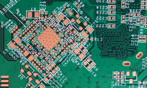
6 Layers FR4 Medical Equipment PCB Double Sided with OSP Surface Finish
The 6 layers double-sided PCB is made FR4 raw material with finish board thickness of 1.6 mm, which is applied to medical equipments. The total specification of the medical equipment PCB is 79 * 30 mm, while the minimum aperture, line trace and space are 0.1 mm.

How to get quick quotation?
| Step 1 Please send us Gerber file with these format: .CAD / .Gerber / .PCB / .DXP / .P-CAD, etc | ||||||||||||||||||||
| Step 2 Also please provide us the below details for quick quotation: | ||||||||||||||||||||
|
Board material: Fr - 4 / CEM - 1 / CEM - 3 / 22F / Fr - 1 / others |
||||||||||||||||||||
| Material brand: SY / KB / Rogers (optional) | ||||||||||||||||||||
| Material Specification:High Tg / copper based / aluminum based or others (optional) | ||||||||||||||||||||
| Board thickness: 0.1 - 6.0 mm | ||||||||||||||||||||
| Copper thickness: 0.05 Oz - 8 Oz ( 17 um - 288 um ) | ||||||||||||||||||||
| Surface Treatment: OSP / ENIG / HASL / Lead Free HASL / Immersion Tin / Immersion Sin | ||||||||||||||||||||
| Color of solder mask and silk print: Green / red / blue / black / white / yellow ,etc | ||||||||||||||||||||
| Board size and quantity | ||||||||||||||||||||
|
If you don't have Gerber file, please provide us the imfomation as step 2 or post your PCB Board to us for clone.
|
||||||||||||||||||||
|
SAMPLE:
|
||||||||||||||||||||
|
||||||||||||||||||||
| Item | Details |
| Max layer count | 20 L |
| Max board thickness | 6.0 mm |
| Max aspect ratio | 10 : 1 |
| Max copper thickness | 6 OZ |
| Max dimension | 600 * 700mm |
| Min thickness of 4 layers PCB | 0.4 mm |
| Min hole / pad | 0.15 / 0.35mm |
| Hole location accuracy | + / - 0.05mm |
| PTH hole tolerance | + / - 0.05mm |
| Min line width and line space | 0.065 / 0.065mm |
| Surface treatment |
HASL / HASL lead free, OSP
Immersion gold/silver/tin, gold plating (hard gold and soft gold),
silver plating, tin plating, platinum plating, carbon ink,
ENEPIG (electroless nickel - electroless palladium - immersion gold) |
| Layer count | Sample lead time/workday | Batch lead time/workday |
| 1-2L | 2 | 6 |
| 4L | 5 | 8 |
| 6L | 5 | 9 |
| 8L | 6 | 10 |
| 10L | 8 | 10 |
| 12L | 8 | 12 |
| 14L | 10 | 15 |
| 16L | 10 | 18 |
| 18-40L (Up to difficulty) | at least 18 | at least 24 |
| P.S. For HDI, Blind/Buried Hole PCB: Regular Lead Time + 3 workdays | ||
| AOI (Automated Optical Inspection) | Impedance control |
| Automatic short-circuit testing | Metallographic microscope |
| RoHS detector | Fly probe/ fixture mold |
| Dielectric tester | Visual inspection |
Now send us your inquiry, and you will be replied within 8 hours!
Little knowledge - Multilayer PCB Board
Multilayer printed circuit boards (Multilayer PCBs) represented the next major evolution in fabrication technology.
A very sophisticated and complex methodology came from the base platform of double sided plated.
This methodology would again allow circuit board designers a dynamic range of interconnects and applications.
Multilayer PCB board were essential in the advancement of modern computing, and their basic construction and fabrication are similar to micro chip fabrication on a micro size.
The range of material combinations is extensive from basic epoxy glass to exotic ceramic fills, and it can be built on ceramic, copper, and aluminum. Also, blind and buried vias are commonly produced in multilayer pcb manufacturing, along with pad on via technology.
|
|
6 Layers FR4 Medical Equipment PCB Double Sided with OSP Surface Finish Images |