| Sign In | Join Free | My xxjcy.com |
|
- Home
- Products
- About Us
- Quality Control
- Contact Us
- Get Quotations
| Sign In | Join Free | My xxjcy.com |
|
Brand Name : LEFANG
Model Number : RM0002L093
Certification : ISO9001, ISO14001, ISO/TS16949, SGS, UL, RoHs,OHSAS18000
Place of Origin : Shenzhen,China
MOQ : 1 Piece
Price : Negotiable
Payment Terms : T/T, Western Union, Paypal, MoneyGram
Supply Ability : 290, 000 sqm Per Month
Delivery Time : 2-10 work days
Packaging Details : Inner: Vacuum Packing; Dry Packing out Packing
Raw material : Fr - 4
Layer count : 2 Layer
Board thickness : 1.6 mm
Copper thickness : 1 Oz / 35 µm
Surface treatment : OSP
Solder mask : Green
Board size2104 * 105 mm4.56 * 58.83 mm : 106 * 75 mm
Min. Aperture : 0.3 mm
Line Trace Width/Space : 0.1 / 0.1 mm
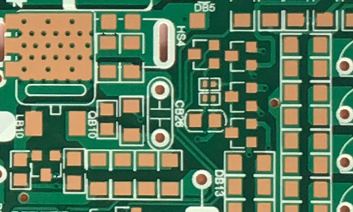
RoHS Printed Circuit Board for Power Bank Board High TG230 Double Sided Board
For the high TG230 double sided PCB Board, the board thickness is 1.6 mm and the copper thickness is 1 OZ / 35 µm. Also, the surface treatment of this double sided PCB Board is OSP. Its minimum aperture is 0.3 mm, and the line width and space is 0.1 mm.

![]()
| Step 1 Please send us Gerber file with these format: .CAD / .Gerber / .PCB / .DXP / .P-CAD, etc | ||||||||||||||||||||
| Step 2 Also please provide us the below details for quick quotation: | ||||||||||||||||||||
|
Board material: Fr - 4 / CEM - 1 / CEM - 3 / 22F / Fr - 1 / others |
||||||||||||||||||||
| Material brand: SY / KB / Rogers (optional) | ||||||||||||||||||||
| Material Specification:High Tg / copper based / aluminum based or others (optional) | ||||||||||||||||||||
| Board thickness: 0.1 - 6.0 mm | ||||||||||||||||||||
| Copper thickness: 0.05 Oz - 8 Oz ( 17 um - 288 um ) | ||||||||||||||||||||
| Surface Treatment: OSP / ENIG / HASL / Lead Free HASL / Immersion Tin / Immersion Sin | ||||||||||||||||||||
| Color of solder mask and silk print: Green / red / blue / black / white / yellow ,etc | ||||||||||||||||||||
| Board size and quantity | ||||||||||||||||||||
|
If you don't have Gerber file, please provide us the imfomation as step 2 or post your PCB Board to us for clone.
|
||||||||||||||||||||
|
SAMPLE:
|
||||||||||||||||||||
|
||||||||||||||||||||
| Item | Details |
| Max layer count | 20 L |
| Max board thickness | 6.0 mm |
| Max aspect ratio | 10 : 1 |
| Max copper thickness | 6 OZ |
| Max dimension | 600 * 700mm |
| Min thickness of 4 layers PCB | 0.4 mm |
| Min hole / pad | 0.15 / 0.35mm |
| Hole location accuracy | + / - 0.05mm |
| PTH hole tolerance | + / - 0.05mm |
| Min line width and line space | 0.065 / 0.065mm |
| Surface treatment |
HASL / HASL lead free, OSP
Immersion gold/silver/tin, gold plating (hard gold and soft gold),
silver plating, tin plating, platinum plating, carbon ink,
ENEPIG (electroless nickel - electroless palladium - immersion gold) |
Lead Time
| Layer count | Sample lead time/workday | Batch lead time/workday |
| 1-2L | 2 | 6 |
| 4L | 5 | 8 |
| 6L | 5 | 9 |
| 8L | 6 | 10 |
| 10L | 8 | 10 |
| 12L | 8 | 12 |
| 14L | 10 | 15 |
| 16L | 10 | 18 |
| 18-40L (Up to difficulty) | at least 18 | at least 24 |
| P.S. For HDI, Blind/Buried Hole PCB: Regular Lead Time + 3 workdays | ||
| Board Brand | ITEQ, SY, Isola. Rogers, Arlon, Nelco, Taconic, Hitachi, KB,etc |
| Potion | Rohm & Haas, Atotech, Umicore |
| Printing Ink | Taiyo, Rongda |
| Dry Film | Asahi, Dupont, Etertec |
Now send us your inquiry, and you will be replied within 8 hours!
Little knowledge - Single Sided PCB
Single sided PCB contains only one layer of conductive material, where components are focused on one side, and the other side of the wire is concentrated.
Single sided PCB are the best choice for low density designs. They are easily designed and quickly manufactured to serve as the most cost effective platform in the industry.
For surface finishes, single sided boards are available for Organic surface protectant (OSP), Immersion Silver, Tin, and Gold plating along with both leaded or lead-free Hot Air Solder Level (HASL), with operating temperatures range from 130℃ to 230℃.
|
|
High TG230 Two Layer Power Bank PCB Board , Rohs Printed Circuit Boards Images |